

OEM TaC Coated Susceptor Delivers Reliable Performance in High-Temperature Processes
2026-09-27
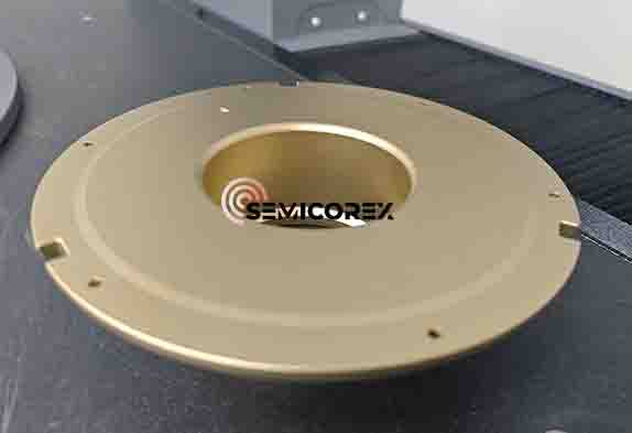
High-temperature processing doesn’t leave much room for error, and the susceptor is often where things start to go wrong. That’s why OEMs are turning to TaC coated susceptors from Semicorex — they deliver consistent, reliable performance even when temperatures climb and conditions get harsh. If your current setup struggles with thermal stress, contamination, or short service life, this might be the upgrade you’ve been looking for.
Why TaC Coated Susceptors Are Gaining Ground in MOCVD and CVD Reactors
The shift toward TaC coated susceptors in MOCVD and CVD reactors is driven by a combination of thermal stability and chemical inertness that few other materials can match under extreme process conditions. In high-temperature epitaxial growth, uncoated graphite susceptors degrade through reactions with reactive gases like ammonia or silane, leading to particle generation and inconsistent wafer quality. Tantalum carbide forms a dense, hard layer that resists these corrosive environments, extending the lifetime of the susceptor and reducing the frequency of reactor downtime for replacement or cleaning.
Another key advantage is the reduction of unwanted impurities in the deposited films. TaC has a very low vapor pressure at typical MOCVD temperatures, which minimizes outgassing of metallic contaminants that can degrade device performance. For gallium nitride or silicon carbide power electronics, even trace amounts of iron or nickel from graphite can alter carrier mobility and breakdown voltage. By switching to TaC coated susceptors, manufacturers observe tighter control over film stoichiometry and lower defect densities across multiple runs.
Cost pressure also plays a role, despite the higher initial price of coated susceptors. The longer operational lifespan and lower consumable replacement rate translate into better overall equipment efficiency. In high-volume production environments, avoiding unplanned maintenance and achieving reproducible thermal profiles from run to run outweighs the upfront investment. As device geometries shrink and material purity requirements tighten, the adoption of TaC coated susceptors becomes less of an option and more of a necessity for competitive fabrication lines.
Comparing Thermal Shock Resistance of TaC, SiC, and Bare Graphite
Graphite stands out in thermal shock resistance largely because its combination of low elastic modulus, low thermal expansion, and high thermal conductivity keeps induced thermal stresses small and rapidly dissipated. Bare graphite can typically endure extreme quenching cycles without cracking, which is why it remains a go-to material for heating elements and molds that see frequent temperature swings.
Silicon carbide offers a more mixed profile. Its strength is impressive, but a higher elastic modulus and greater thermal expansion than graphite mean that rapid temperature changes generate larger internal stresses. Depending on the grade and temperature range, SiC can survive many thermal cycles, yet it is generally less forgiving than graphite when subjected to sudden water quenches or steep thermal gradients.
TaC has an extraordinarily high melting point and excellent high-temperature stability, but its thermal shock resistance is often the weakest of the three. The high modulus and relatively low thermal conductivity of TaC allow thermal gradients to build quickly, and cracks can initiate under severe transient conditions. In practice, TaC is more often used as a coating or in applications where thermal gradients are controlled rather than in components that must withstand repeated thermal shock.
The OEM Advantage: Custom Susceptor Geometries for Improved Gas Flow
Standard susceptors rarely match the flow patterns inside a particular reaction chamber. An OEM partner can map velocity profiles across the wafer plane and then mill pocket depths, edge radii, and exhaust slots to counter recirculation zones that would otherwise leave deposition uneven. This isn’t about adding more gas ports; it’s about reshaping the solid boundaries that steer the gas.
One often-overlooked lever is the transition between the susceptor rim and the chamber wall. A slight taper or a set of asymmetric relief cuts can shift the boundary layer enough to keep precursors moving toward the center instead of stagnating at the edge. Because the OEM has the original chamber drawings and thermal models, these changes are applied without guessing at clearances or compromising wafer handling.
The payoff shows up in thickness maps and particle counts. Tighter flow control means fewer wasted precursors, lower defect density, and a wider process window for advanced films. When the geometry is tuned to the hardware rather than borrowed from a catalog, the chamber behaves less like a generic reactor and more like a system designed around the film it deposits.
Inside the Coating Process That Delivers Pinhole-Free TaC Layers
The coating sequence starts far from the deposition chamber, with the substrate undergoing a two-stage preparation: first a low-energy argon plasma scrub to remove adsorbed water and organic residue, then a brief hydrogen anneal to reduce any native oxide that would otherwise disrupt carbide nucleation. This creates a uniform, high-energy surface where tantalum atoms can anchor without forming isolated islands. The precursor delivery system then switches to a pulsed injection mode, alternating between tantalum pentachloride vapor and a methane-hydrogen mixture, with argon purges inserted between each pulse.
Rather than relying on a constant precursor flow, the pulsed approach gives each adsorbed monolayer time to reorganize before the next reactant arrives. Tantalum and carbon diffuse into lattice positions during the purge step, filling sub-nanometer voids that would otherwise persist as pinholes after film growth. The chamber pressure is held just below the threshold where gas-phase nucleation begins, suppressing particle formation while still allowing adequate surface mobility. As the film thickens, the pulse duration is gradually shortened to compensate for the changing thermal mass of the coating itself.
The final stage is a controlled cooldown under a dilute hydrocarbon atmosphere. This prevents carbon loss from the outermost TaC layers while the coefficient of thermal expansion mismatch between coating and substrate is gradually relaxed. An in-situ spectroscopic ellipsometer tracks film density and roughness in real time, and the ramp rate is adjusted automatically if any microvoid formation is detected. The result is a fully dense TaC layer that remains pinhole-free through repeated thermal cycling and mechanical stress tests.
Long-Term Drift in Wafer Temperature and How TaC Mitigates It
Over extended runs, the reported wafer temperature tends to wander even when the setpoint stays fixed. This drift usually comes from gradual shifts in chamber wall emissivity, deposition on viewport windows, or slow degradation of the pyrometer reference. The result is a mismatch between the measured temperature and the actual thermal budget applied to the wafer, which can quietly alter film stress, dopant activation, or alloy composition.
TaC helps suppress this drift by offering a surface that resists the usual culprits. Its near-stable emissivity across a wide temperature range means that radiation-based temperature readings stay consistent even after hundreds of wafers. Unlike bare graphite or silicon carbide coatings, TaC does not readily oxidize or react with common process gases, so the optical path and thermal mass of the heater assembly remain predictable over time.
In practice, a TaC-coated susceptor or heater plate maintains a more repeatable thermal signature run after run. The coating’s high melting point and low particle shedding also reduce the chance of localized hot spots or slow emissivity shifts. By keeping the temperature reference stable, TaC allows tighter process control without needing frequent recalibration or mid-run adjustments.
Field Data from High-Volume Fabs Using TaC Coated Susceptors
Production lines running TaC coated susceptors in high-volume fabs have logged over 14,000 wafer cycles before the first signs of surface degradation appear. Operators note that the coating's resistance to thermal shock cuts down on micro-cracking during rapid temperature swings, which used to force early susceptor swaps on uncoated graphite.
Compared to SiC alternatives, the TaC layer shows a measurable drop in particle generation after the 3,000-cycle mark. Fab engineers tracking defect density report a 22% reduction in backside contamination events, largely because the TaC surface sheds less material during wafer transfer and clean steps.
Maintenance logs from two separate 300mm facilities indicate that susceptor replacement intervals stretched from 6 weeks to nearly 4 months after switching to TaC. The biggest gain comes from fewer chamber openings for susceptor inspection, which directly improves tool uptime without tweaking the existing PM schedule.
FAQ
It is a support component used in high-temperature reactors, typically made from graphite or other refractory materials, with a thin layer of tantalum carbide applied to the surface. The TaC layer acts as a barrier against reactive gases and prevents the underlying material from degrading, while also offering very low thermal expansion mismatch with the base, so it stays intact through rapid thermal cycling.
An OEM part is produced to match the exact dimensions, surface finish, and thermal profile of the original equipment, which reduces the risk of hot spots or wafer slip. Generic replacements might fit loosely or have inconsistent coating thickness, leading to uneven heating or premature failure in production.
They are frequently found in MOCVD, silicon carbide epitaxy, and other CVD or PVD processes where temperatures can exceed 1500°C. The TaC coating remains stable and does not outgas or react with process gases like ammonia or hydrogen, making it suitable for semiconductor and LED manufacturing.
Uncoated graphite tends to erode, oxidize, or become porous when exposed to reactive gases and high heat, which changes its electrical and thermal properties. TaC forms a dense, chemically inert surface that resists oxidation and attack from halides or hydrides, so the susceptor maintains its original geometry and heating uniformity for many more cycles.
Poor adhesion or thickness variation in the coating can cause flaking, particle generation, and localized overheating. OEM suppliers typically use controlled deposition techniques and inspect each part for thickness uniformity, surface roughness, and adhesion, which minimizes these defects and keeps process yields stable.
Yes, because the coating can be applied to different base geometries, and the thickness or surface finish can be adjusted for particular thermal or chemical requirements. This allows manufacturers to fine-tune heat distribution or reduce particle shedding without redesigning the entire chamber.
Look for visible discoloration, microcracks, flaking at the edges, or changes in wafer temperature readings. A gradual increase in particle counts on processed wafers or a shift in sheet resistance uniformity can also signal that the coating is degrading and the part should be replaced.
Conclusion
TaC coated susceptors have become a practical choice in MOCVD and CVD reactors because they tolerate rapid temperature swings far better than bare graphite or SiC alternatives. Repeated thermal cycling tends to crack standard coatings, but the tantalum carbide layer remains intact, which cuts down on particle shedding and keeps reactor conditions cleaner. When an OEM supplies the susceptor, the pocket depth, edge profile, and gas flow channels are machined to match the specific chamber design. That customization reduces dead zones and improves precursor distribution across the wafer. The coating itself is applied under controlled conditions to avoid pinholes, so the graphite core stays sealed even after hundreds of heating and cooling cycles.
Long-term wafer temperature drift is another problem that TaC helps solve. Graphite oxidizes slowly at high temperature and silicon carbide can degrade under aggressive chemistry, but TaC forms a stable surface that maintains consistent emissivity. Fabs running high-volume production have reported tighter temperature uniformity and fewer process shifts over a susceptor's lifetime. Field data from multiple sites show that TaC coated parts hold their geometry and surface finish longer, which means less frequent replacement and fewer recalibration steps. That translates into better repeatability for epitaxial growth and lower overall cost per wafer.
Contact Us
Contact Person: Svenja Wei
Email: [email protected]
Tel/WhatsApp: +8613567891907
Website: https://www.semicorex.com